


Samsung Electronics, the world’s largest memory chipmaker, announced Wednesday it has developed a dynamic random access memory (DRAM) chip that is capable of a data processing speed of 1.3 gigabytes per second-the fastest in the world.
Currently, multimedia phones that support 3D graphics and digital cameras with a picture resolution of over 5 mega-pixels need a DRAM with a memory capacity of 256 megabits. The new chip can handle 512 megabits of information, while consuming less energy: 1.8 volts of electricity per second, compared with the older DRAM at 2.5 to 3 volts.
Samsung naturally expects the new chip to improve the functions of its third-generation (3G) handsets, which it plans to begin manufacturing in the second half of the year.
세계 최대 메모리칩 제조업체 삼성전자가 지난 수요일 초당 1.3 기가바이트의 데이터를 처리할 수 있는 세계 최고속 D램을 개발했다고 발표했다.
현재 3D 그래픽과 해상도 5 메가픽셀 이상의 디지털 카메라가 장착된 멀티미디어 핸드폰에는 256메가 용량의 D램을 필요로 한다. 이 새로 나온 칩은 1.8볼트의 전력으로 512메가의 정보를 처리할 수 있어 초당 2.5-3 볼트의 전력이 필요한 기존의 D램보다 에너지 면에서도 더 효율적이다.
삼성 측에서는 이 새로운 칩으로 올 하반기부터 생산에 들어가려고 계획하고 있는 3세대 핸드폰의 성능이 향상될 수 있을 것으로 기대하고 있다.
capable of …: …할 수 있는
per second: 1초당
second half of the year: 하반기
<제공: (주)능률교육 http://www.EnglishCare.com>


오피니언 많이 본 뉴스
-
1
[전문가기고] 텅스텐, K방산 및 K반도체의 약한 고리
-
2
[ET시론]대한민국 AI의 심장, AI 데이터센터
-
3
[데스크라인] 폐쇄적 정책의 후과
-
4
[사설] 금융사 보안공시에 파격 인센티브 주라
-
5
[김장현의 테크와 사람] 〈104〉인공지능 시대의 문해력
-
6
[사설] 구글 제재, 앱 생태계 회복 출발점돼야
-
7
[기고] 세계 6위 국력의 이면, 글로벌 R&D 특별법 제정이 시급하다
-
8
[GEF 스타트업 이야기] 〈89〉기부 시장의 '매슈 이펙트'와 컴포저블 거버넌스의 시대
-
9
[기고] 과징금의 목적은 처벌이 아니라 예방이다
-
10
[부고] 박정훈(서울 송파갑 국회의원)씨 부친상


브랜드 뉴스룸
-
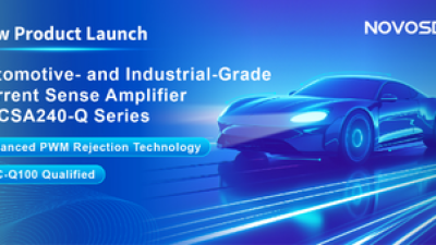 노보센스노보센스, PWM 고주파 과도 간섭 난제 극복…차량용 전류 감지 증폭기
 디에스앤지디에스앤지, 'AI EXPO KOREA 2026' 참가 성료… AI 전 생애주기 아우르는 통합 솔루션 선봬
 에이블스토어[컴퓨텍스 2026]이제 CCTV 영상 분석도 AI가…시놀로지 '시멘틱 검색'
 -
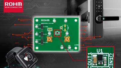 로옴세미컨덕터코리아로옴, 초소형 실장 면적 구현한 승강압 전원 레퍼런스 기판 개발
 AIPD[에듀플러스]“AI 잘 쓰는 것보다 올바르게 쓰는 것이 먼저”…우리 아이 AI 자격검정 'AIPD 주니어' 주목
 글로쿼드텍[人사이트]장기수 글로쿼드텍 대표 “글로벌 전기차·모빌리티 충전 솔루션 선도기업 도약”
 -
 토마토시스템토마토시스템, 美서 헬스케어 플랫폼 특허 출원…“의료기관·보험사 공략”
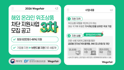 위고페어한국지식재산보호원, '2026년 3차 해외 온라인 위조상품 차단 지원사업' 모집 시작
 시큐어링크시큐어링크, 중소기업기술정보진흥원 AI 초격차 R&D 사업 최종 선정
 -
 인아그룹'자동화 산업의 새로운 가능성'…인아그룹 전국 7개 도시 세미나 페어 개최
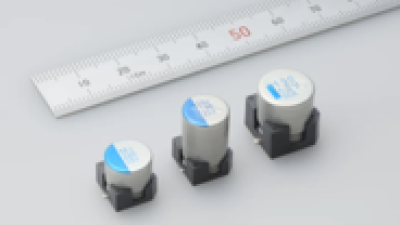 태양유전태양유전, 대전류·고내압 대응 차량용 하이브리드 알루미늄 전해 커패시터 HVX(-K)·HTX(-K) 시리즈 출시
 와이즈스톤'AI 어떻게 믿지?'…와이즈스톤, 국제인공지능대전서 AI 품질 서비스 공개
 -
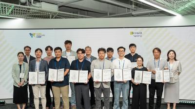 다래전략사업화센터다래전략사업화센터, 제18기 기보벤처캠프 성료
 한국무라타전자무라타, 제품 데이터베이스 전 제품 대상 API 서비스 제공…73개 제품 카테고리로 확대
 슈퍼솔루션슈퍼솔루션, NVIDIA HGX B300 공랭식 서버 재고 확보로 안정적 공급망 강화
 -
 포시에스전자문서·전자계약 1위 포시에스, “기업가치 제고로 주주환원 강화” 계획 공시
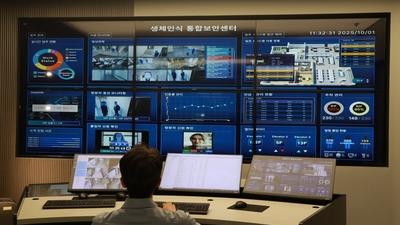 유니온커뮤니티유니온바이오메트릭스, 중동서 보안 프로젝트 잇단 수주
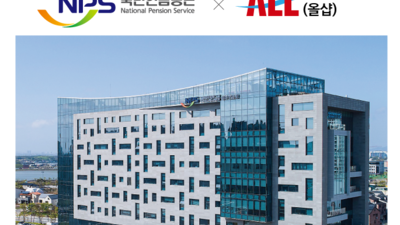 씨앤에프시스템씨앤에프시스템, 국민연금 치매재산관리서비스에 ALL# ERP 공급
 -
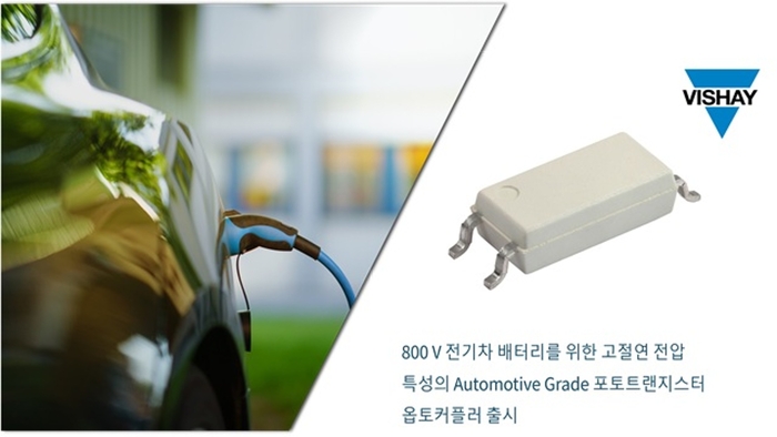 비쉐이비쉐이, 800V 전기차 배터리용 고절연 전압 Automotive Grade 포토트랜지스터 옵토커플러 출시
 가온아이가온아이, 서울기록원 차세대 디지털 아카이브 시스템 구축 수행
×
![]()